What We Offer
Photonic Integrated Circuits Design
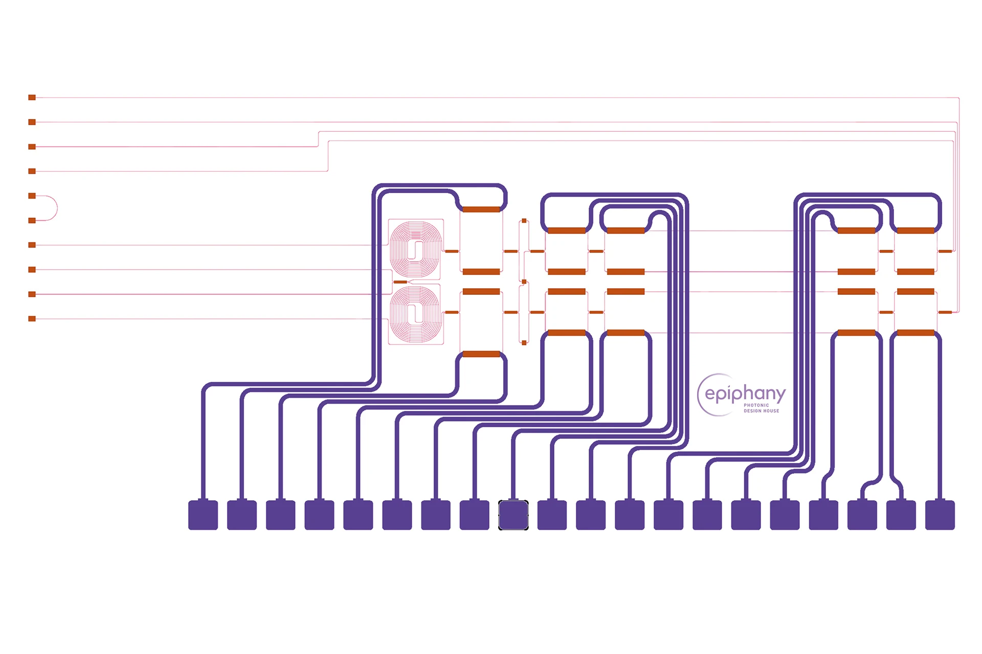
With over 35 years of experience in PIC Design, Epiphany accompanies you from your first idea to the production of your personalized PIC.
Our Process Explained
Epiphany's process often begins with a feasibility review, assessing the projects scope and technical viability. We then seamlessly move into building block design, where physical simulations and parameter analysis are needed to optimize key components. In the schematic design phase, circuit simulations and layer-vs-schematic verification ensure design integrity and are used as additional verification steps of the PIC design. Once validated, the final step is to process the chip layout, with packaging and testing in mind. Here, future test protocols are established.
Guiding You at Every Stage
Whether you're starting from scratch or already have a plan, we can guide you through the process — helping you choose the right idea, the right platform, or supporting your existing concept. We work with a wide range of technologies, PIC platforms, and design frameworks, giving you the flexibility to select what best fits your application. We're here to support you at any stage, or throughout the entire journey, depending on your needs and preferences.
Our Added Value
Your Vision, our Expertise

Flexibility
As a fabless company, we work across a wide range of technologies, PIC platforms, and design frameworks—giving you the flexibility to choose what fits your application best.

Independence
As an independent design house, we provide unbiased advice, follow your preferences, and offer guidance at any stage of the process or whenever you need it.

Experience
Our team brings hands-on experience from across the photonics ecosystem—from foundry engineers to design and software specialists, with a strong understanding of real-world application needs.
More About PIC Materials
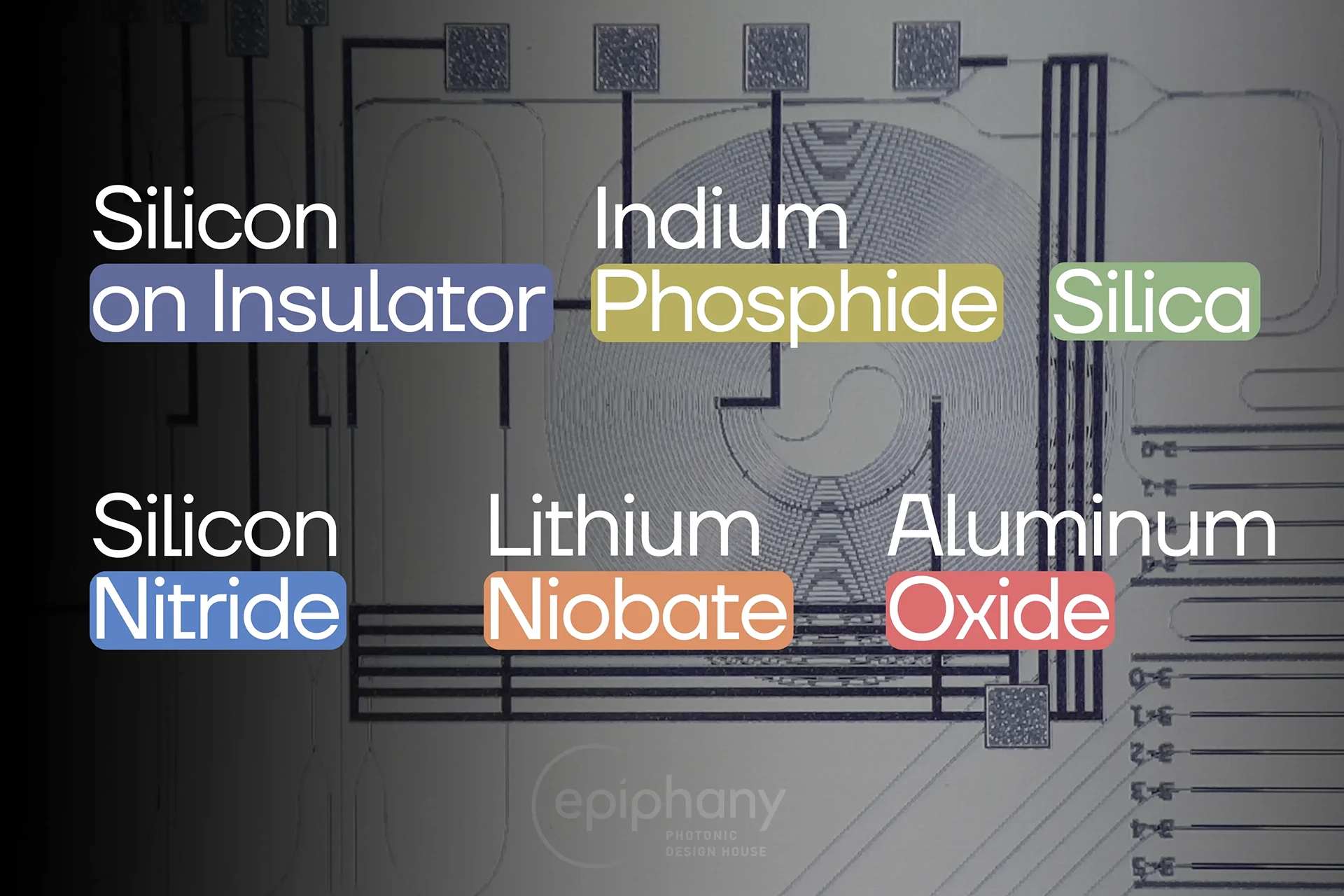
A Guide to PIC Technologies
Explore the strengths and use cases of different photonic integrated circuit (PIC) technologies—and find out which one fits your application best.
The Answers to your Questions
Frequently Asked Questions
What is Photonic Integrated Circuit (PIC) design?

Photonic Integrated Circuit (PIC) design is the process of creating optical circuits on a semiconductor chip. These circuits integrate components such as waveguides, modulators, detectors, and lasers to manipulate light on-chip. PIC design involves system architecture, optical simulations, layout creation, and preparation of fabrication-ready design files for photonic foundries.
What does a photonic design house do?
A photonic design house provides engineering services for the design and development of PICs. This includes translating system requirements into optical circuit architectures, selecting foundries and packaging partners, designing photonic components, performing simulations, and preparing layouts compatible with foundry fabrication and packaging processes. Epiphany supports companies in developing PIC designs from first ideas (such as early architecture definition) all the way to fabrication-ready layouts.
What photonic platforms can PICs be designed on?
PICs can be designed on several material platforms depending on the application and requirements. Common platforms include Silicon on Insulator (SOI), Silicon Nitride (SiN), Indium Phosphide (InP), Lithium Niobate (LNOI), Aluminum Oxide (AlOx), etc. Each platform offers different advantages in terms of loss, integration capability, modulation speed, wavelength range and costs. Learn more about PIC platforms on our Guide to PIC Technologies. As a fabless design house, Epiphany works across multiple PIC platforms, enabling cross-platform design and technology evaluation.
What is a photonic PDK?
A photonic Process Design Kit (PDK) translates the capabilities and processes of a foundry onto design software (so-called electronic design automation, EDA). PDK can provide different capabilities from basic layout instruction and design rules to libraries that contain already validated photonic components and even simulation models. Often it allows designers to build circuits using components that are known to be compatible with the manufacturing process. Epiphany is also supporting foundries with PDK development and maintenance. Learn more about our Foundry Enablement service here.
What is hybrid or heterogeneous photonic integration?
Hybrid or heterogeneous integration combines different materials or photonic technologies within a single system to achieve functionalities that cannot be realized in a single platform alone. For example, low-loss waveguides in Silicon Nitride may be combined with active components such as lasers or modulators implemented in Indium Phosphide or Lithium Niobate. System-level photonic design must consider optical coupling, packaging constraints, and fabrication compatibility when combining different technologies.
When should a company outsource PIC design?
Companies typically outsource PIC design when they lack in-house photonics design expertise or capacity and want to accelerate their development. External design houses can support early architecture development, component design, layout implementation, and foundry preparation, allowing teams to focus on system development and product integration. At Epiphany Design, the team performs many tape-outs every month across different PIC platforms and applications, which provides broader practical experience across foundries, technologies, and design approaches.
What is included in a photonic chip design project?
A PIC design project typically includes the following stages:
- System architecture and specification definition
- Optical circuit design and simulation
- Subsystem design using foundry building blocks and custom components
- Layout implementation using the foundry PDK
- Design rule checking and verification
- Preparation for fabrication (tape-out)
Depending on the project, Epiphany may also support system modeling, integration strategy, and preparation for multi-project wafer (MPW) runs or dedicated runs.
How long does it take to design a photonic integrated circuit?
Design timelines depend on the circuit complexity and maturity of the concept. Simple PICs may take a few weeks to design, while complex multi-functional chips may require several months. Additional time may be required for simulation, verification, and preparation for foundry tape-out.
Do I need a PDK to design a photonic integrated circuit?
While not strictly necessary, most modern PIC designs are developed using a Process Design Kit (PDK) provided by the photonic foundry. The PDK contains validated building blocks, process rules, and simulation models that ensure designs are compatible with the fabrication processes.
Epiphany works with multiple foundry PDKs and supports design flows adapted to each platform.
Can a photonic design be migrated between foundries?
In some cases, a design can be adapted to another foundry or platform, but this typically requires redesign of components and layout elements. Different foundries use different waveguide geometries, component libraries, and fabrication rules. As a result, migration usually involves revalidation of optical performance and design rule compliance. Foundry building blocks must generally be replaced, or re-designed if necessary. Cross-platform design expertise is often required to perform this process efficiently. To make the transfer of designs easier between different foundries and technologies Epiphany works with Design Modules to give their/our customers the flexibility they need.
What tools are used for photonic integrated circuit design?
PIC design typically uses photonic design environments similar to Electronic Design Automation (EDA) tools. These tools allow schematic design, layout generation, and design rule checking. They are often combined with simulation tools for optical performance and system verification.
Epiphany uses industry-standard photonic design tools and simulation environments to develop fabrication-ready designs from layout, physical layer simulation, circuit simulation to design verification.
Can photonic chips integrate lasers and detectors on the same chip?
Yes, certain photonic platforms such as Indium Phosphide support monolithic integration of lasers, modulators, and detectors. Other platforms may combine active and passive devices through hybrid or heterogeneous integration approaches.
How can I start a photonic integrated circuit design project with Epiphany?
A typical project starts with a technical discussion about the application, performance targets, and preferred technology platform.
Based on this information, the design scope can be defined, including system architecture, simulation needs, and the target fabrication route. The outcome is usually a design plan leading to a fabrication-ready PIC layout.
How much does it cost to fabricate a photonic integrated circuit?
The cost of PIC fabrication depends on the platform, foundry, chip size, and whether the design is part of a multi-project wafer run or a dedicated wafer.
Multi-Project Wafer (MPW) runs significantly reduce the cost of early prototypes. Later project stages are usually more expensive than earlier ones.
Fabrication costs more than design, packaging and testing often costs more than fabrication, dedicated runs cost more than MPW runs, and so on.
What is a Multi-Project Wafer (MPW) Run?
A multi-project wafer (MPW) run is a shared fabrication approach where different chip designs from multiple users are combined onto a single wafer and processed together in one manufacturing cycle. Instead of each project requiring its own dedicated (and more costly) fabrication run, participants share the costs of the manufacturing. Their individual designs are placed on different sections of the same mask set, allowing everyone to benefit from the same standardized process flow and proven building blocks. This makes MPW runs especially attractive for prototyping photonic integrated circuits, testing new concepts, or validating designs before scaling up.
When should a company work with a photonic design house?
Companies often collaborate with photonic design houses when developing a new photonic technology, evaluating fabrication platforms, or when internal teams lack specialized PIC design expertise or capacity.
External design support can accelerate development and reduce risk when preparing designs for fabrication. A thorough planning and design phase reduces the number of expensive iterations needed to make a product.
What Else We Offer
More Services from Epiphany

Production Support
As an independent design house, Epiphany offers tailored support to help you choose the ideal foundry, packaging & testing partner for your project.

Foundry Enablement
Epiphany empowers foundries by offering PDK development, building block design, test and characterization support, and could act as partner in managing customer interactions.

Hybrid Laser Design Module
Rather than starting your photonic design from scratch, this solution represents a ready-to-integrate module, enabling you to focus on advancing other aspects of your PIC project.
Contact Us
Our Journey Together
We can accompany you every step of the way, from your first idea to your final PIC. Our advantage of being a fabless design house allows us to tailor each step to your individual needs.


