Photonic Technology
Indium Phosphide
Indium phosphide is a photonic integrated circuit (PIC) material suited for active functionalities. Beyond passive light routing, it can generate, amplify and detect light. Read on this page to learn more about indium phosphide characteristics, applications, and its comparison to other PIC platforms.
Learn about Indium Phosphide
Why use this Technology
Overview
Indium Phosphide (InP) is a well-established material for discrete optoelectronic components. It has been used commercially for several decades for laser diodes and photodetectors operating in the O- and C- bands, particularly for optical fiber communications. Recently, InP is becoming increasingly important as a generic platform for photonic integrated circuits. This is due to its ability to enable monolithic integration of all active components, especially lasers and semiconductor optical amplifiers, as well as high-speed photodetectors and modulators, together with waveguides and other passive components.
Characteristics
InP has a direct bandgap with energy corresponding to telecom wavelengths and high electron mobility, which makes it an ideal platform for high-power light sources and high-speed modulators for long-haul and high data rate optical links.
In combination with other monolithically integrated active and passive functionalities, it is promising for a larger scale integration of PICs with many components on a single chip, such as multi-channel coherent transmitters and receivers for optical communications. However, InP waveguides have higher propagation losses than SOI or SiN waveguides.
The larger waveguide cross-section and lower refractive index contrast (about 3.3) of InP waveguides compared to SOI result in larger bend radii of 100 µm or more and, hence, a larger footprint in a PIC.
In applications where monolithic integration is not crucial, InP active components can be heterogeneously or hybridly integrated with more compact passive SOI or SiN PICs instead by means of bonding, edge coupling or micro-transfer printing.
Applications
Besides applications in telecom and datacom, the InP platform can be used for automotive LiDAR and sensing, such as distributed sensing, and potentially in consumer electronics or wearable medical devices. When co-integrated with other PIC platforms, it can be used for integrated lasers with improved characteristics, for applications in metrology or sensing.
Bring your PIC project to life
At Epiphany Design, we work with all PIC material platforms and always advise our customers on the best choice for their particular applications. When it comes to indium phosphide photonics, we know how to make the most of its strengths to create solutions across a wide range of use-cases. We specialize in PIC Design, but also provide support at all stages of PIC development when needed.
Learn about Different Photonic Technologies
Explore Photonic Materials

Overview
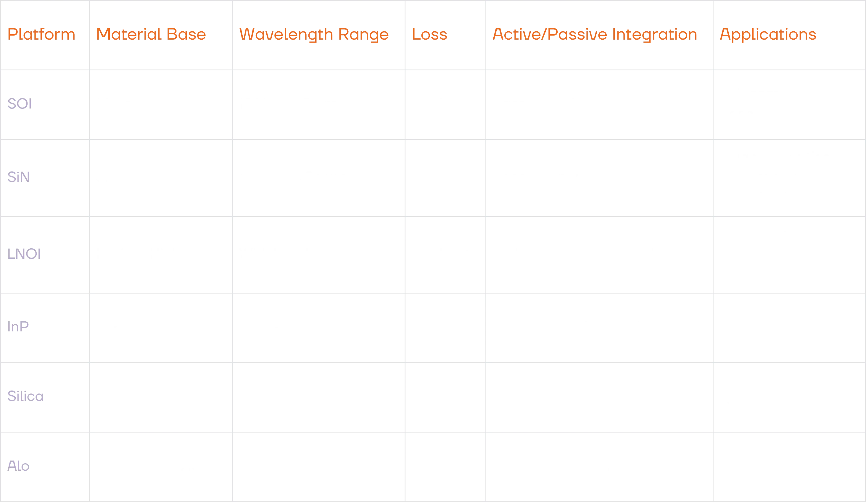
Use the comparison table at the bottom of this page to get an overview of all the materials & and their specifications.

Silicon Nitride
Silicon Nitride is a photonic integrated circuit platform known for its low propagation loss and broad transparency.

Silicon on Insulator
Silicon On Insulator (SOI), also known as Silicon Photonics (SiP) technology, is the most mature platform for photonic integrated circuits.
Lithium Niobate
LNOI is a PIC material valued for high-speed, linear electro-optic modulation and wide transparency from visible to mid-infrared wavelengths.

Aluminum Oxide
Coming up soon! Send us a message if you’d like to receive more information before this part of the guide is published.

Silica
Coming up soon! Send us a message if you’d like to receive more information before this part of the guide is published.
Check out the Comparison Table
Compare PIC Technologies
Contact Us
Our Journey Together
We can accompany you every step of the way, from your first idea to your final PIC. Our advantage of being a fabless design house allows us to tailor each step to your individual needs.


