Photonic Technology
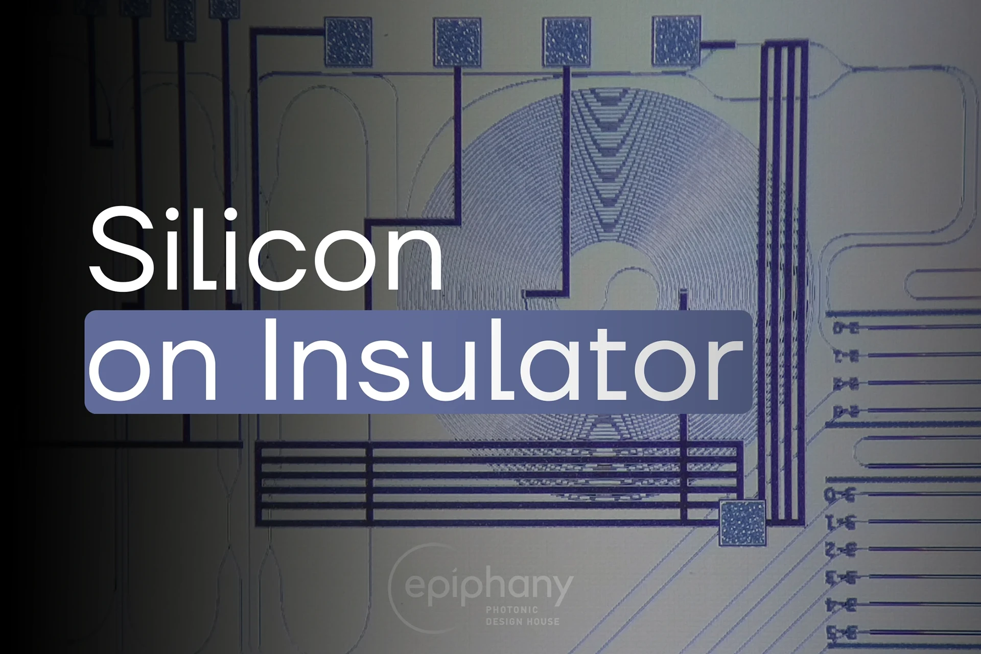
Silicon on Insulator
Silicon on Insulator (SOI), also known as Silicon Photonics (SiP) technology, is the most mature platform for photonic integrated circuits (PICs). On this page, you can learn more about the characteristics and applications of SOI, as well as how it compares to other PIC platforms.
Learn about Silicon on Insulator
Why use this Technology
Overview
Silicon Photonics (SiP) is the most mature and widely adopted photonic integrated circuits platform. It leverages the many advantages of integrated photonics by offering a high density of devices and mass producibility due to its compatibility with CMOS technology. By using the established infrastructure of the semiconductor industry, silicon photonics enables the integration of photonic and electronic components on a single chip, offering unmatched scalability and cost-effectiveness.
Characteristics
Silicon photonics leverages the mature silicon manufacturing infrastructure of the semiconductor industry. By itself, silicon cannot be used for light generation as it has an indirect band gap, but it can be used for other active optical components such as modulators and detectors when combined with other materials. When activated by doping silicon with germanium, it can be used to make both high-speed modulators and photodetectors operating at frequencies of 70 GHz and beyond.
Among the common PIC platforms, silicon has the highest refractive index contrast and the tightest fabrication tolerance. This enables unrivaled integration density with bending radii of a few micrometers and high yield. To connect optical fibers to SiP chips, grating couplers are often used, but also edge couplers become more and more available sometimes with additional silicon nitride layers. In silicon polarization control is relatively straightforward by implementing polarization splitters and then combiners. Thermo-optic phase shifters can switch as fast as 10s of kHz with a power consumption in the 10s of mW.
The typical operating wavelengths for SiP are 1310 nm and 1550 nm, but wavelengths between 1200 nm and 6500 nm are, in principle, accessible. Propagation losses are usually moderate, around 3 dB/cm or lower depending on the specific waveguide cross-section and wavelength. Due to its intrinsic two-photon absorption, silicon often cannot support higher optical powers of more than a few 10s of mW.
Because silicon cannot be used as a gain medium, lasers cannot be directly built within silicon. Therefore, external lasers or co-integrated gain materials must be used through hybrid or heterogeneous integration. However, when integrated with gain materials, SiP can be used for the feedback section of a hybrid integrated laser for improved performance.
Applications
Thanks to its scalability, integration density, and CMOS compatibility, Silicon Photonics (SiP) is a key enabler for a wide range of applications. SiP is especially common for transceivers, interconnects, and signal processing in telecom and datacom applications. It is also increasingly used in emerging quantum communication applications such as Quantum Key Distribution (QKD). In addition, silicon photonics has become the main platform for LiDAR thanks to its efficient grating couplers and small footprint, possibly in combination with silicon nitride for optical power handling.
The SiP technology is unique for (co-)integrating optical and electronic circuits on a single chip or substrate, reducing costs and power consumption. It is primarily used in data communication, sensors, and high-performance computing.
Bring your PIC project to life
At Epiphany Design, we work with all PIC material platforms and always advise our customers on the best choice for their particular applications. When it comes to silicon photonics, we know how to make the most of its strengths to create solutions across a wide range of use-cases. We specialize in PIC Design, but also provide support at all stages of PIC development when needed.
Learn about Different Photonic Technologies
Explore Photonic Materials

Overview
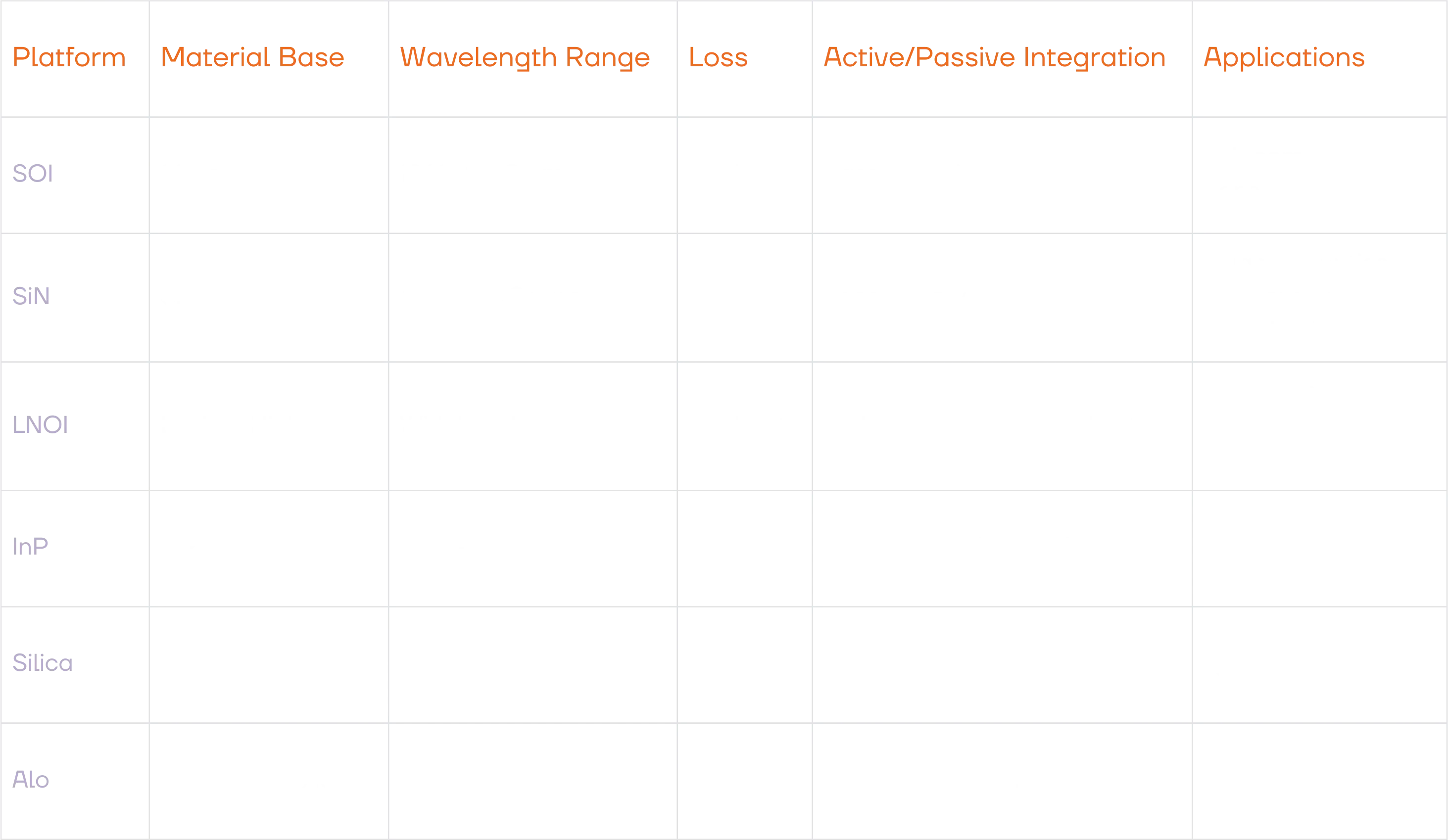
Use the comparison table at the bottom of this page to get an overview of all the materials & and their specifications.

Silicon Nitride
Silicon Nitride is a photonic integrated circuit platform known for its low propagation loss and broad transparency.

Indium Phosphide
Indium phosphide is a photonic integrated circuit material suited for active functionality. Beyond passive light routing, it can generate, amplify and detect light.
Lithium Niobate
LNOI is a PIC material valued for high-speed, linear electro-optic modulation and wide transparency from visible to mid-infrared wavelengths.

Aluminum Oxide
Coming up soon! Send us a message if you’d like to receive more information before this part of the guide is published.

Silica
Coming up soon! Send us a message if you’d like to receive more information before this part of the guide is published.
Check out the Comparison Table
Compare PIC Technologies
Contact Us
Our Journey Together
We can accompany you every step of the way, from your first idea to your final PIC. Our advantage of being a fabless design house allows us to tailor each step to your individual needs.


